The Effects of Increasing the Aspect Ratio of GaAs Backside Vias
To support the current trend in industry of working towards higher via densities which could shrink via dimensions, we report […]
To support the current trend in industry of working towards higher via densities which could shrink via dimensions, we report […]
Unaxis solutions for plasma-enhanced chemical vapor deposition (PECVD) silicon nitride (SiNx) are used extensively in the production of GaAs devices.
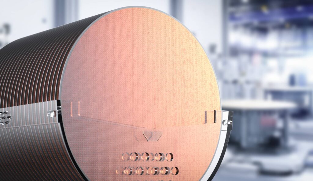
Cornell University’s Nanoscale Science and Technology Facility (CNF) recently took delivery of a VERSALINE® deep silicon dry etching system. The comprehensive
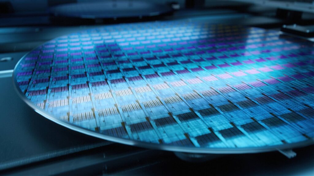
Conventional reactive ion etching (RIE) has generally been used for selective etching of GaAs over AlGaAs. However, there is a