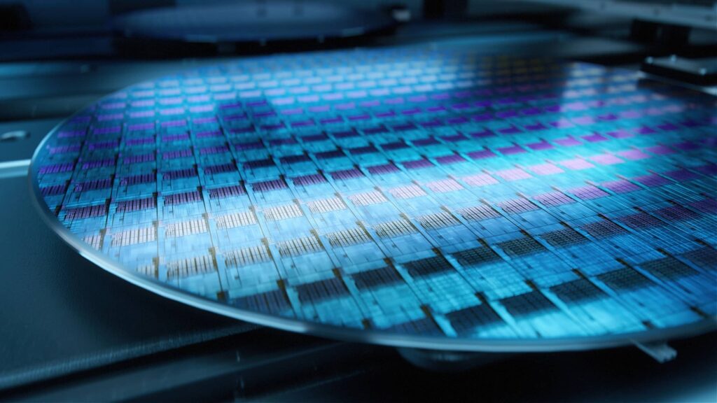
Optimization of Low Stress PECVD Silicon Nitride for GaAs Manufacturing
Unaxis solutions for plasma-enhanced chemical vapor deposition (PECVD) silicon nitride (SiNx) are used extensively in the production of GaAs devices. […]
Unaxis solutions for plasma-enhanced chemical vapor deposition (PECVD) silicon nitride (SiNx) are used extensively in the production of GaAs devices. […]
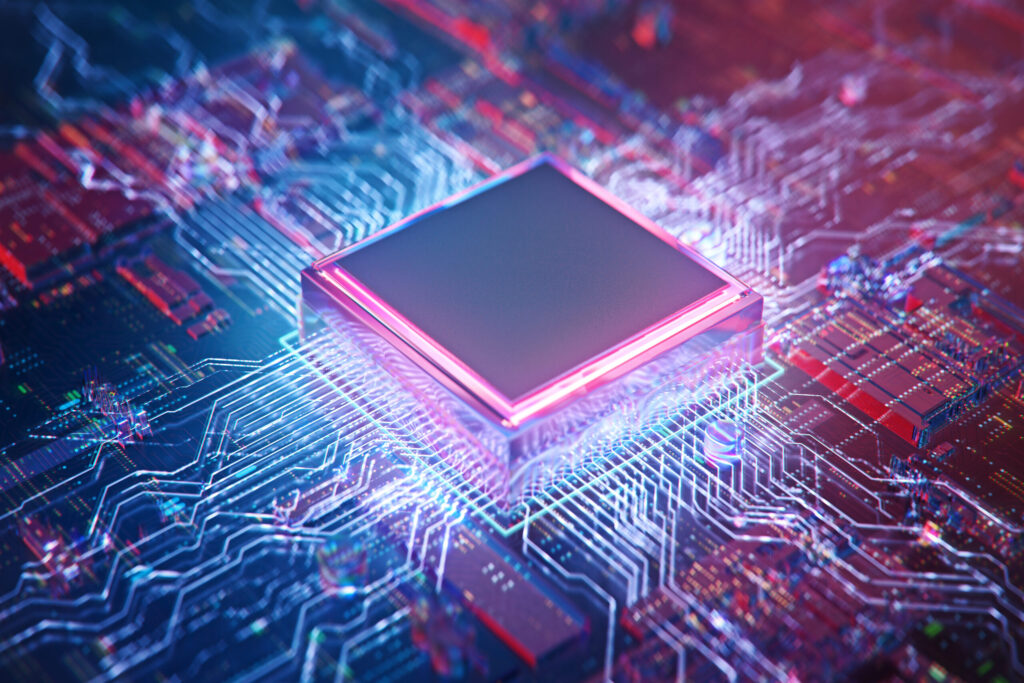
Today’s information age requires moving and manipulating vast amounts of data at the highest possible speeds with the lowest possible
Plasma processing plays a vital role in semiconductor manufacturing, especially in ultra-large-scale integrated fabrication, by providing precise control over the
SEMICON Japan, Tokyo, December 15, 2022 — Plasma-Therm, a leading manufacturer of plasma-process equipment for the semiconductor and compound semiconductor
SEMICON Europa, Munich, Germany, November 15, 2022—Plasma-Therm, a leading manufacturer of plasma-process equipment for the semiconductor and compound semiconductor markets,
SEMICON West, San Francisco, Calif., July 12, 2022—Plasma-Therm, a leading manufacturer of plasma-process equipment for the semiconductor and compound semiconductor
Conventional reactive ion etching (RIE) has generally been used for selective etching of GaAs over AlGaAs. However, there is a
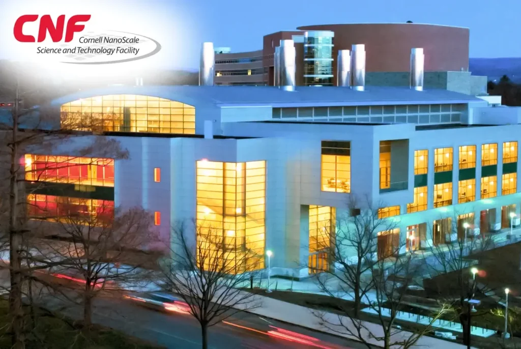
Cornell University’s Nanoscale Science and Technology Facility (CNF) recently took delivery of a VERSALINE® deep silicon dry etching system. The comprehensive
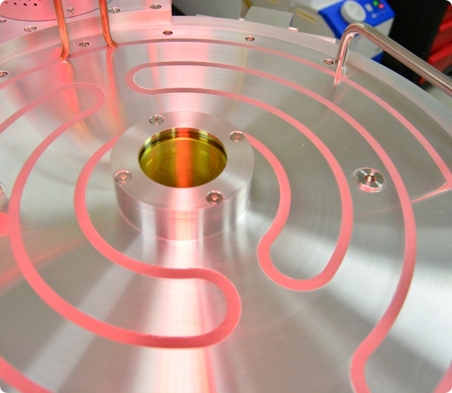
To support the current trend in industry of working towards higher via densities which could shrink via dimensions, we report
There is no excerpt because this is a protected post.